- electronics
IC fabrication flow
How a chip is made, from a bare silicon wafer to a packaged die - oxidation, lithography, etching, doping, deposition, polishing and yield. A first-principles learning page.
datasheet // ic-fabrication-flow
- images
- 2
- videos
- 0
- formats
- png
- text
- 654 words · 3 min read
- studio
- /studio (gallery)
- topics
-
- oxidation ×1
- yield ×1
On this page0%
A learning page: standard process physics from the textbooks listed at the bottom, with figures computed from the formulas shown. It makes no claim of new research results, and the process constants are typical textbook values, not those of any particular factory.
Intuition
A chip is built like a layered city, one thin layer at a time, on a polished silicon disc called a wafer. Each layer follows the same loop: put down a film, print a pattern on it with light, then remove or modify the film where the pattern says so. Repeat that loop dozens of times with different patterns and the transistors and wires appear.
School level
The main building steps are:
- Oxidation: heating silicon in oxygen grows silicon dioxide, an excellent insulator.
- Lithography: light through a mask patterns a light-sensitive resist.
- Etching: removes material wherever the resist does not protect it.
- Doping: adds small, controlled amounts of boron, phosphorus or arsenic to change silicon’s conductivity.
- Deposition: adds films of metal, oxide or silicon (chemical vapour deposition, sputtering, atomic layer deposition).
- Polishing (CMP): flattens the surface so the next layer prints sharply.
- Test and packaging: the wafer is cut into dies, which are tested and put in packages.
Front-end steps build the transistors; back-end steps build the stack of copper wiring above them.
College level
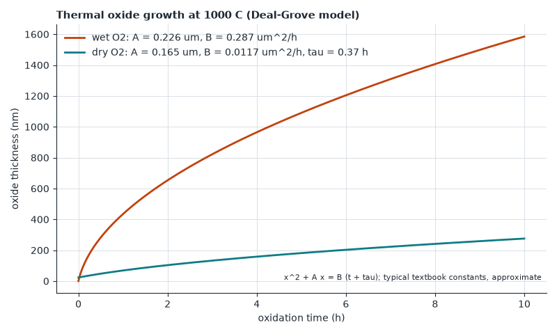
Oxide growth (Deal-Grove). Oxygen must diffuse through the existing oxide and react at the silicon surface, so thickness x follows
x2 + A x = B (t + τ).
For short times growth is linear, x ≈ (B/A)(t + τ), limited by the surface reaction. For long times it is parabolic, x ≈ √(B t), limited by diffusion. Typical textbook constants at 1000 °C are A = 0.226 µm and B = 0.287 µm2/h for wet oxidation, and A = 0.165 µm, B = 0.0117 µm2/h, τ = 0.37 h for dry (figure 1). Wet oxide grows far faster, dry oxide is denser.
Ion implantation. The implanted dose Q lands in a roughly Gaussian profile, N(x) = Q / (√(2π) ΔRp) exp(−(x − Rp)2 / (2 ΔRp2)), centred on the projected range Rp; an anneal then repairs the damage and activates the dopant while diffusion spreads it.
Yield. If defects land randomly with density D on a die of area A, the Poisson model gives Y = e−A D, and Murphy’s model Y = ((1 − e−A D) / (A D))2 allows for defect clustering (figure 2).
Advanced
- A modern flow has hundreds of steps; overlay (aligning each layer to the one below, to a few nanometres) and process control matter as much as any single step.
- Copper wiring is made by the damascene process: etch trenches in oxide, fill with copper, polish flat, repeat for each metal level.
- Yield falls exponentially with area, which is why very large chips cost disproportionately more and why splitting one design into smaller chiplets is attractive.
Where this shows up
- Every processor, memory and sensor chip.
- Process design kits and the design rules that circuit designers must follow.
Check yourself
- Why does oxide growth slow down as the film thickens? Answer: oxygen has to diffuse through more oxide to reach the silicon, so the process turns from reaction-limited (linear) to diffusion-limited (parabolic).
- A die of 2 cm2 is made at D = 0.5 per cm2. What is the Poisson yield? Answer: e−1 ≈ 37 %.
- The die of question 2 is split into two dies of half the area. What is the Poisson yield now? Answer: A D falls from 1 to 0.5, so Y = e−0.5 ≈ 61 %, which is 1.65 times better. Because yield is exponential in area, each halving multiplies it by eA D / 2.
Read next
- J. D. Plummer, M. D. Deal and P. B. Griffin, Silicon VLSI Technology.
- S. A. Campbell, Fabrication Engineering at the Micro- and Nanoscale.
- G. S. May and C. J. Spanos, Fundamentals of Semiconductor Manufacturing and Process Control.