- electronics
VLSI circuit design
From a single CMOS inverter to a chip - logic levels, noise margin, dynamic power, the energy-delay trade-off and the digital design flow. A first-principles learning page.
datasheet // vlsi-circuit-design
- images
- 2
- videos
- 0
- formats
- png
- text
- 572 words · 3 min read
- studio
- /studio (gallery)
- topics
-
- digital ×1
- power ×1
On this page0%
A learning page: standard circuit theory from the textbooks listed at the bottom, with figures computed from the formulas shown. It makes no claim of new research results, and the device parameters are illustrative.
Intuition
Digital circuits decide between two voltages, “high” and “low”, and keep deciding even when the signals are a bit noisy. The simplest decider is the inverter, which turns a high into a low and a low into a high. Chain millions of them into gates and you can compute anything. The art of design is keeping them fast, small and cool.
School level
- A CMOS inverter has a p-type MOSFET connecting the output to the supply and an n-type connecting it to ground. A high input turns the n-type on (output low); a low input turns the p-type on (output high).
- Only one of the two conducts once the output has settled, so a CMOS gate draws almost no current at rest.
- Every time a gate switches it charges or discharges the capacitance of the wires and gates it drives, and that costs energy.
College level
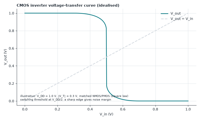
The inverter’s voltage-transfer curve (figure 1) is flat at the two rails and falls sharply near VDD/2 for matched transistors. The steep middle gives the noise margins: how far an input can drift from a rail and still be read correctly.
Power. A full charge-and-discharge cycle of a node of capacitance C moves charge C VDD from the supply and dissipates energy C VDD2 in total, so the dynamic power of a circuit is
Pdyn = α C VDD2 f,
with activity factor α and clock frequency f, plus leakage power.
Delay. The alpha-power law (Sakurai-Newton) gives gate delay td ∝ C VDD / (VDD − VT)α, with α between 1 and 2. Lowering VDD cuts energy quadratically but slows the gates, which is the basis of dynamic voltage and frequency scaling (figure 2).
Analog. A common-source amplifier has a small-signal gain of about −gm RD, and the intrinsic gain of a single transistor is gm ro. Feedback around a high-gain amplifier makes a stable, precise operational amplifier.
Advanced
- Digital design flow: specify, write RTL (hardware description language), simulate, synthesise to gates, place and route, verify timing, check power and design rules, then tape out to the foundry.
- Timing closure: every path from one register to the next must settle within one clock period, including variation from voltage, temperature and manufacturing.
- Low-power design: clock gating, power gating of idle blocks and multiple supply voltages.
Where this shows up
- Processors, memory interfaces, sensor read-out chips and radio front ends.
- Electronic design automation tools and cell libraries.
Check yourself
- A circuit switches at 1 GHz with α = 0.1, C = 1 nF total and VDD = 1 V. What is its dynamic power? Answer: 0.1 × 10-9 × 12 × 109 = 0.1 W.
- If VDD is cut from 1.0 V to 0.7 V, by what factor does switching energy per operation fall? Answer: to 0.72 = 0.49 of its value, about half.
- Why does a CMOS gate draw so little current at rest? Answer: in each steady state one of the two transistors is off, so there is no direct path from supply to ground apart from small leakage.
Read next
- N. H. E. Weste and D. M. Harris, CMOS VLSI Design.
- B. Razavi, Design of Analog CMOS Integrated Circuits.
- J. M. Rabaey, A. Chandrakasan and B. Nikolić, Digital Integrated Circuits.